Readers seeking reliable silicon carbide wafer suppliers can compare a range of 4H SiC wafers designed for high-temperature, high-power, and high-frequency applications. This guide presents five well-suited options, highlighting who each product serves best, why it’s a strong choice, and any limitations to consider. Ideal buyers include researchers, engineers in power electronics, and developers needing robust, high-temperature substrates.
Summary table of chosen products
| Product | Best For | Key Benefit |
|---|---|---|
| Silicon Carbide Wafer Monocrystalline Substrate 4H Conductive Type 0.35mm (1in) | Experimental research, high-temperature work | High-temperature tolerance and strong breakdown field |
| Silicon Carbide Wafer Monocrystalline Substrate 4H Conductive Type 0.35mm (2in) | Advanced lab experiments, small-scale prototyping | Higher operating temperature capability |
| SiC Wafers – 4H Conductive & Semi-Insulating (6″ x 0.625mm) | Power electronics, high-frequency devices | Thermal conductivity and dual type options |
| 4H Silicon Carbide Wafer Monocrystalline Substrate 0.35mm (1in) | Power electronics research, stability-focused studies | Excellent thermal management |
| SiC Wafers – 4H Conductive & Semi-Insulating (5x10x0.35mm) | High-power, demanding environments | Temperature resilience and versatile types |
Silicon Carbide Wafer Monocrystalline Substrate 4H Conductive Type 0.35mm (1in)

Best for early-stage experimental work, this 0.35mm thick monocrystalline SiC wafer supports high-temperature testing and high-voltage experiments. The 4H structure provides a wider bandgap, enabling operation beyond 400°C. It also offers a strong breakdown field compared to silicon, making it suitable for devices that demand elevated voltage handling. Choose this if you are validating novel designs in a compact lab setup and need reliable high-temperature performance. A potential limitation is the smaller size, which may constrain large-scale production experiments.
Silicon Carbide Wafer Monocrystalline Substrate 4H Conductive Type (2in)
Better for mid-size lab work, this 2-inch conductive 4H SiC wafer supports experimental use in scientific research with a higher working diameter. The wider bandgap allows higher operating temperatures exceeding 400°C, suitable for advanced electronic applications. Its high breakdown field strength makes it apt for high-voltage device development. A caveat is that the 2-inch format may require compatible handling tools and equipment in your facility.
SiC Wafers – 4H Conductive & Semi-Insulating (6″x0.625mm)

Best for high-frequency and high-power applications, these 4H wafers come in both conductive and semi-insulating types. They offer exceptional thermal conductivity for effective heat transfer, supporting longer device lifespans under high temperatures. The bandgap is about three times that of silicon, enabling operation beyond 400°C. Consider this option if you need dual-type versatility, but note that larger wafer sizes may demand more specialized processing equipment.
4H Silicon Carbide Wafer Monocrystalline Substrate 0.35mm (1in)
Best for power electronics research, this 0.35mm-thick 4H wafer emphasizes premium thermal conductivity. Such cooling efficiency helps maintain stability during high-temperature operation. The 4H structure offers a bandgap roughly three times that of silicon, enabling operation beyond 400°C. Choose this if your project prioritizes heat management and temperature resilience, but be aware of its suitability for smaller-scale experiments rather than mass production.
SiC Wafers – 4H Conductive & Semi-Insulating (5x10x0.35mm)

Best for demanding environments, these 4H SiC wafers come in conductive and semi-insulating types. They deliver exceptional thermal conductivity and operate over 400°C, supporting high-temperature, high-power applications. They are a solid choice when dual-type versatility is needed for parallel testing. A limitation to monitor is that the precise dimensions may require exact tool alignment during processing.
High Wear-Resistant Silicon Carbide Round Wafer (20x10mm, 2pcs)
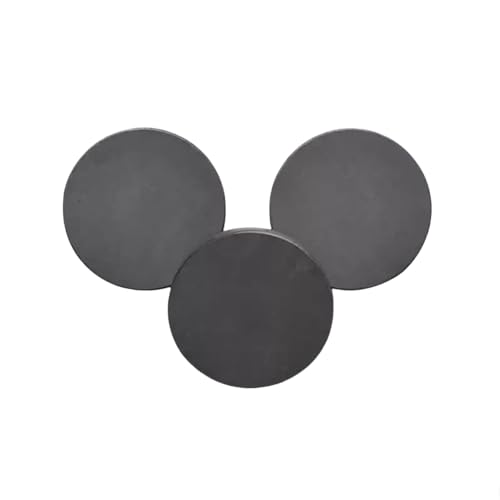
Best for specialized industrial testing requiring wear resistance and heat tolerance, this non-pressure ceramic sheet offers high hardness and excellent thermal conductivity. Its erosion resistance to solvents adds versatility for harsh environments. It’s a niche option best suited for durability-focused experiments or durable tooling studies, not for standard device fabrication. Consider size and form-factor compatibility with your existing equipment.
SiC Wafers – 4H Conductive & Semi-Insulating (10x10x0.35mm)
Best for parallel testing and scalable layouts, these 4H wafers provide conductive and semi-insulating types with good thermal performance. Their ability to operate above 400°C suits demanding environments, especially where high-frequency and high-power devices are evaluated. A limitation is that larger wafers may require careful handling and specialized processing lines to prevent damage during processing.
Buying Guide: Key Considerations for Silicon Carbide Wafers
What wafer dimensions do you need? Smaller diameters are appropriate for early prototypes and lab experiments, while larger wafers support more extensive research and higher-volume development. Consider thickness as well; 0.35mm is common for flexible testing, but thicker options may offer better mechanical stability.
What type matters most—conductive or semi-insulating? Conductive wafers enable easier electrical characterization, whereas semi-insulating types help minimize parasitic conduction and improve device isolation. Some products offer both, enabling side-by-side comparisons.
How important is the operating temperature? SiC wafers with wider bandgaps withstand higher temperatures, often beyond 400°C. This is critical for high-temperature electronics and power devices where thermal management is essential.
What about thermal management? Look for wafers with high thermal conductivity and structures designed to improve heat dissipation. Efficient cooling extends device life and maintains performance under stress.
How robust is the supply chain? Consider supplier reliability, batch consistency, and availability of compatible processing tools. For research labs, steady access to substrates reduces project downtime and helps maintain testing continuity.
Frequently Asked Questions
- What is the main use for silicon carbide wafers? They are used for high-temperature, high-power, and high-frequency electronics research and device prototyping due to their wide bandgap and thermal properties.
- Why choose 4H silicon carbide substrates? The 4H polytype offers a wide bandgap, strong breakdown field, and good thermal conductivity, which are advantageous for high-voltage and high-temperature devices.
- What does conductive vs semi-insulating mean? Conductive wafers have higher electrical conductivity for easier testing, while semi-insulating wafers reduce unwanted conduction for better isolation in devices.
- Are there size limitations to consider? Yes. Smaller wafers are easier for initial experiments; larger wafers enable larger-scale testing but require compatible handling and processing tools.
- How do temperature ratings affect device design? Higher operating temperatures require materials with wider bandgaps and effective thermal management to prevent performance loss.
- What should I verify before purchasing? Confirm wafer type (conductive or semi-insulating), diameter, thickness, and compatibility with your processing equipment and measurement setups.
Add a Comment